
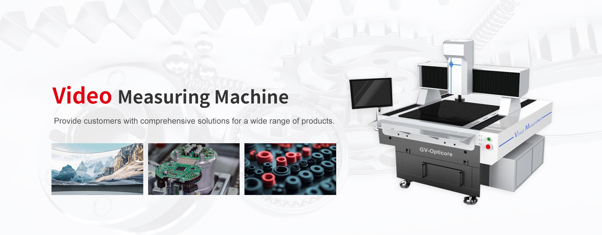
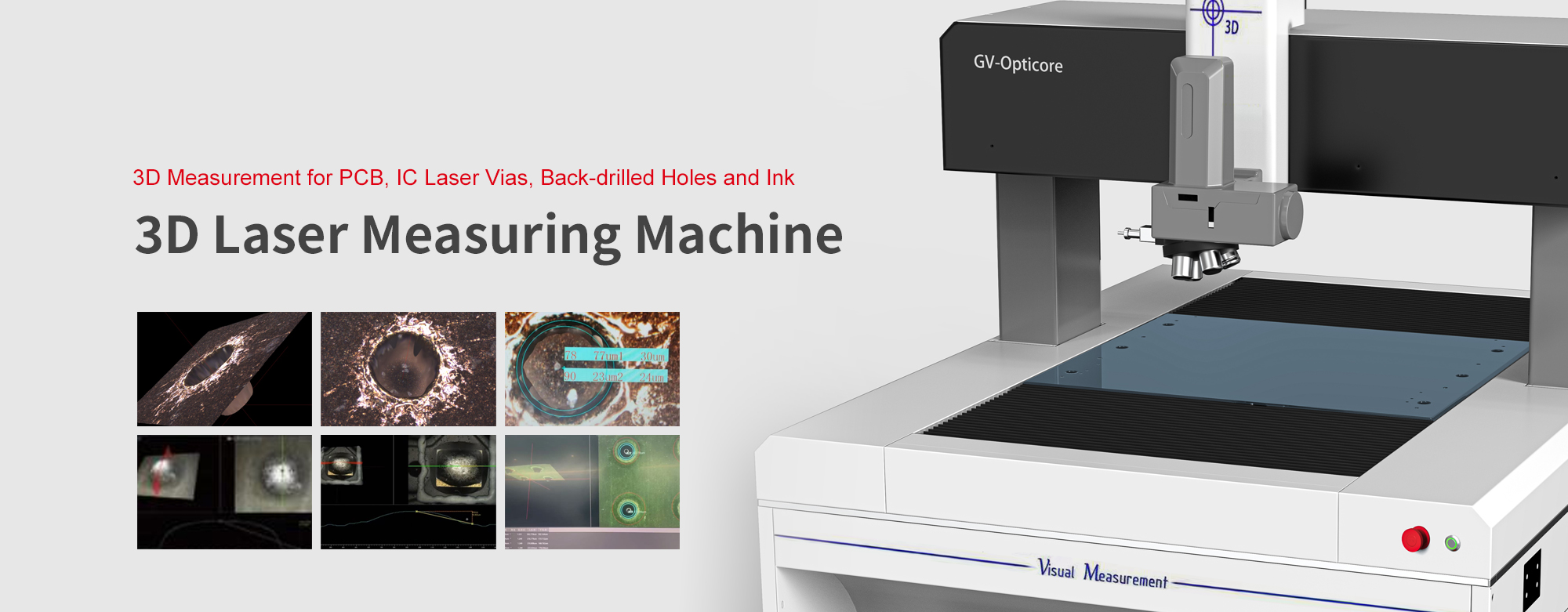
Product Introduction
Driven by the semiconductor industry roadmap's rapid pursuit of shrinking transistors, PCB manufacturers are developing smaller, denser, thinner high-density interconnect (HDI) and multi-chip module (MCM) substrates. The ContourSP Large Panel Metrology System with metrology capabilities is a nanoscale precision measuring instrument specially designed to measure each layer of PCB boards during the manufacturing process, ensuring minimal recipe development time, maximum throughput, longest uptime and lowest cost per measured panel in production.

Product Advantages
1. Unique Features for Maximum Productivity
Highest Throughput: More than 2x faster than the previous generation system. Many new features: 1) Dynamic Signal Segmentation (DSS) 2) Re-measurement function 3) Topography scanning for wafer bow compensation 4) Coordinated file import, ESD, panel ID reader 5) Operator access control based on Vision64. Recipe portability for multi-tool/multi-function factory deployment.
2. High Resolution and High Precision
With its new anti-vibration system design and patented Wyko Vertical Scanning Interferometry (VSI), the contour system with strain gauge function performs highly accurate 3D Critical Dimension (CD) measurements at nanometer resolution. This feature enables Contours to perform multiple tasks simultaneously as a powerful surface texture metrology instrument and an easy-to-use defect detection tool.
3. Simplified Interface Increases Inter-run Consistency
4. Core components are supplied by well-known American brand companies.